
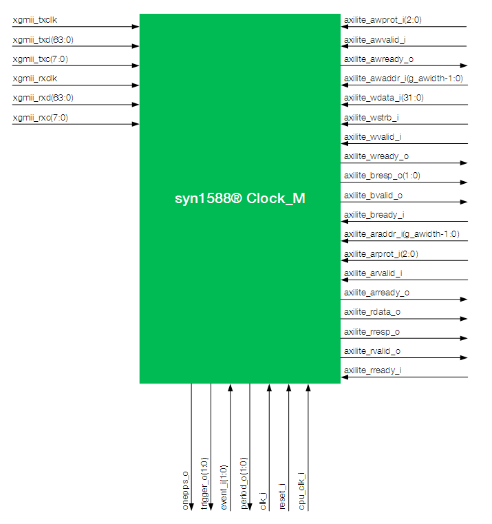
The syn1588® Clock_M IP core family provides highly accurate IEEE1588 compliant clock synchronization functions. The syn1588® Clock_M IP cores are suited for direct integration to an Ethernet MAC. Either one or up to four network interfaces can be connected. A large variety of network line speeds are supported. There is an AXI4 Lite CPU interface for communication with the host processor executing the PTP Stack.
The syn1588® Clock_M IP core family offer all functions required to implement a high-accuracy PTP node. The feature-rich architecture allows creating of PTP slave and PTP master nodes. It's sophisticated hardware clock architecture allow fine-grained clock servo control. All published IEEE1588 standards are supported.
A typical application example is the syn1588® PCIe NIC. This standard PCIe Ethernet network interface card is made up of a single FPGA that includes the syn1588® Clock_M IP core as well as the Ethernet MAC and the PCIe interface
Datasheet
syn1588® Clock_M – Information
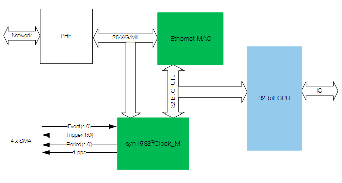
The following figure shows a typical application scenario. Every member of the syn1588® Clock_M IP core family is made up of the following four major function blocks:
- CPU interface
- High-precision hardware clock with clock control
- Network timestamping unit for the selected network speed/type
- Signal Generation
The syn1588® Clock_M IP core is typically accompanied by an Ethernet MAC, an (eventually external) Ethernet PHY and a CPU.
The syn1588® Clock_M IP core family have been designed to fully maintain all real-time tasks completely within the hardware. This includes a special hardware-software interface to ensure proper communication even at high PTP packet rates. The software just implements the high level PTP data flow as defined in the IEEE1588 standard without any real-time constraints. This structure is very important if it comes to manage higher PTP event rates. Note that the term higher rates may be for a standard operating system like windows or Linux already 16 events per second.
syn1588® Clock_M IP core family – Features
- fully synchronous to the system clock
- all registers of the core operate with the rising clock edge
- well commented, structured VHDL source code
- medium footprint and medium I/O count
- AXI4 Lite type slave interface for clock control using independent CPU clock domain
- C/XL/25/X/G/MII netwook interface for IEEE1588 network packet timestamping
- optional user-programmable time stamper unit
- Oregano Systems‘ patented on-the-fly time-stamping (1-step operation)
- 100/1000 Mbit/s link speed support
- 10 Gbit/s link speed support
- 25 Gbit/s link speed support
- 40 Gbit/s link speed support (4x10 Gbit)
- 100 Gbit/s link speed support (4x25 Gbit)
- two timestamp input signals (EVENT function). One EVENT input offers FIFO to capture dense events. This can be used to synchronize to an external GPS-based time source via a 1 PPS signal. Minimum pulse width is 3 x syn1588® clock period.
- Generation of two one-time events (TRIGGER function). One TRIGGER output offers a FIFO to generate dense and precise events. TRIGGERs may be used to start the PERIOD function to allow a precise absolute phase definition in the whole PTP network
- up to four PERIOD outputs allowing generation of periodical signals (clocks) in a frequency range from mHZ to MHz with a resolution of 2-45 ns
- one 1 pulse per second (PPS) output
- generation of digital IRIG-B output stream (DCLS mode IRIG-B000)
- decoding of digital IRIG-B input stream (DCLS mode IRIG-B000)
- generation of interrupts upon external and internal events
- pipelined adder based clock for best synchronization results
- separate receive and transmit timestamp FIFOs
- clock time format compatible to the IEEE1588 standard
- suited for FPGA as well as ASIC implementations
- optional SMPTE 2059 compatible signal generation
syn1588® Clock_M – Resources & Licenses
Resources Utilization
The following table gives a rough overview of the logic resources required for the syn1588® Clock_M IP core. Please note, that the actual implementation figures depends on the selected target technology or FPGA device (family, package, speed grade) as well as the constraints (minimum area or maximum frequency) used for implementing the core.
The following table shows the resources for the syn1588® Clock_M IP core with a single 100/1000 Mbit network interface. All features have been turned on.
- Intel Arria 10: 10AS066K1F40E1SG, 5531 ALM, 6 M20K
- Intel Cyclone V: 5CEBA9F31C8, 2402 ALUTs, 5519 ALM, 6 M20K
- Xilinx Kintex7: XCKU040-FFVA1156-2-E, 7069 LUTs, 9 RAMB36, 1 RAMB18
Licenses
Like for all Oregano Systems‘ IP Cores, there are two ways to license the syn1588® Clock_M IP core.
- technology netlist license for a selected FPGA technology or device
- source code license
When ordering the technology netlist license a gate level netlist for the selected target technology is delivered. The IP core is pre-configured during the netlist generation process and cannot be changed by the user.
When ordering the source code license, the complete VHDL source code of the syn1588® Clock_M core is delivered. Thus the customer may change the IP core as required for the application. The VHDL code is fully synthesizable and requires no special constraints.
More Information
For additional information on our syn1588® products or a detailed quotation please contact us.
Contact Support
Contact us
contact@oregano.at
PHONE
+43 676 84 31 04 -200
+43 676 84 31 04 -300
ADDRESS
Franzosengraben 8
1030 Vienna